Building circuits with the 74HC595 (Part 1)
This is the first of two posts about shift registers. This post focuses on some history behind integrated circuits, how the 74HC595 works, and how to build simple circuits with it. The second post will explore more complex circuits, as well as how shift registers are used today.
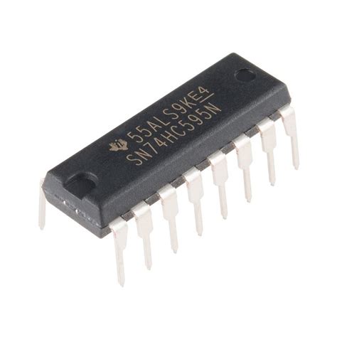
Many general-purpose electronics kits include a few integrated circuits (ICs) in addition to jumper wires, resistors, capacitors, and other electronic circuit components. A common IC included in kits is the 74HC595N, often one manufactured by Texas Instruments (SN74HC595N). After receiving a few of these in various electronics kits, I built several circuits with this shift register to understand how it works.
Background on integrated circuits
Circuits are made up of electrical components, such as resistors, capacitors, transistors, and diodes. While all circuits can be made up of these components, it is often necessary to combine several parts together into a single component, where the parts are closer together, smaller, and merged into a single building block. These circuits are typically etched onto a semiconductor material, such as silicon, and are known as integrated circuits, or ICs for short.
The first IC (an oscillator) was created by Jack Kilby at Texas Instruments in 1958. Robert Noyce invented the first mass-producible IC, fabricating it using the planar process and silicon. IC construction exploded in well-documented fashion at companies such as Fairchild Semiconductor, Intel, and AMD, with Silicon Valley earning its name from the semiconductor material being used to produce these chips.

Source: Wikimedia Commons
Different IC families were developed in the 1960s. The first well-known family, transistor-transistor logic (TTL), was most prevalent in the 1970s and 80s. Computers such as the PDP-11 (of UNIX and C fame) were built using TTL integrated circuits, which derive their name from bipolar junction transistors (BJTs) that perform the digital logic and output.
Later, modern IC development began with metal-oxide-semiconductor (MOS) chips. MOS ICs rely on MOSFETs, transistors with high input impedance that draw much less current than BJTs. While MOS circuits were lower power than TTL circuits, they were not as fast, and didn’t become the default option until Moore’s Law began to make them a more desirable option: as the size of MOSFET transistors decreased, speed increased (and power consumption decreased), as defined by Dennard scaling.

Source: Wikimedia Commons
Complementary metal-oxide-semiconductor chips, or the CMOS family of ICs, use multiple MOSFETs to invert signals. CMOS chips have several benefits for circuits built from them: they draw even less power when not active, as one of the MOFSETs is always off; they do not require pull-up or pull-down resistors to set into a default state; and they are faster than MOS circuits because they can switch more quickly between different states.
Reading IC device numbers
The device number on a chip’s casing provides some information that doesn’t require reading the integrated circuit’s datasheet. Texas Instruments has a useful guide to reading their logic-device part numbers.
The SN74HC595N device number has five components:
-
SN: The standard prefix for TI logic components. The only alternative for this type of logic chip (when purchasing from TI) is SNJ. These distinguish TI circuits that are manufactured for military applications from other circuits. Military-focused circuits are engineered to work more reliably, and have larger ranges of operable temperatures (numbers often cited are 0 to 70 °C for commercial, -40 to 85 °C for industrial, -55 to 125 °C for military). In TI’s case, SNJ denotes that the circuit in question adheres to the US military’s specification for integrated circuits, MIL-PRF-38535.
-
74: This refers to the logic family that our chip is part of. The other option for the number (when considering the 595 circuit) is 54, which is again used to distinguish between military- and commercial-grade chips. The difference between SNJ54 and SN54 is how the part is manufactured and distributed, and you can order either part from TI. The 64 prefix was used for industrial ICs by TI for a short time. Today, it is active for only a few parts. 1
The 7400 logic series was originally introduced by Texas Instruments as a family of digital logic ICs (as opposed to analog ICs). Other manufacturers make 7400-series chips which perform identical functions under similar operating conditions. To identify which chips perform identical functions across (and within) manufacturers, you can remove manufacturer-specific information (the letters) and compare the 7400-series part numbers. For example, Texas Instruments has another IC, the SN74LS595N, which is identical in function (and shape) to the SN74HC595N, and ST’s M74HC595 only differs in specifications (and potentially quality - perhaps better, perhaps worse).
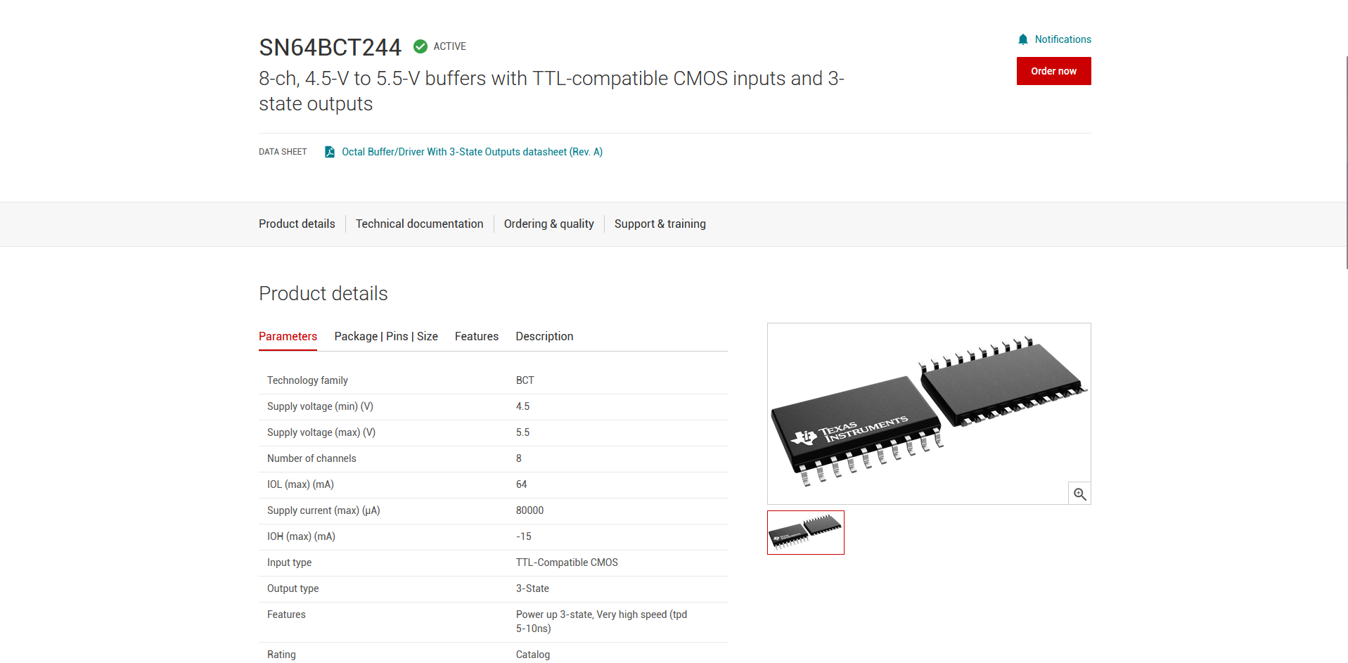
-
HC: The “family” prefix is a more specific indicator of which IC family (TTL, MOS, CMOS, etc.) the circuit belongs to. Depending on how the circuit fits into a larger system, you might choose a low-power option (LS), or one with higher speed (AHC). In this case, HC stands for “high-speed CMOS logic”. The IC uses complementary metal-oxide-semiconductor technology, which provides the benefits of CMOS circuits mentioned earlier when compared with other families like TTL. The 74HC595 also has a higher clock frequency than the same chip from other families (e.g., the LS 595 family has a max. clock speed of 20MHz vs. the HC’s guaranteed maximum operating frequency of 29MHz at 6V (and 42MHz in ideal conditions)).
-
595: The 7400-series has many different functions, each of which is specified by a 2- or 3-digit number. Each number has a unique description which specifies how large the input/output of the circuit is, how many pins it has, what it does generally (timer, oscillator, logic gate), and what it does specifically. There are many types of multiplexers, for example, and each family number distinguishes between them (e.g., the 850 is a “1 of 16 data selector/multiplexer, clocked select” while the 851 is a “1 of 16 data selector/multiplexer” with no clocked select). 2 The short description of the 595 chip is an “8-bit shift registers, serial-in, parallel-out, output latches, output enable”.
-
N: Texas Instruments uses the (in this case) last segment to describe the packaging used. The SN74HC595N is enclosed in a plastic dual-in-line package (PDIP), whose specification describes important physical details about the integrated circuit (you can also find the physical measurements on pg. 37 of the SN74HC595N manual). This information is useful for, e.g., figuring out which footprint you should use for the IC when designing a printed circuit board (PCB) for your system. 3
Reading the datasheet
Reading datasheets is an important skill when designing circuits. While tutorials and articles on the Internet are often useful, there are many ICs (and other components) whose only documentation exists on the website of the company that created them. Additionally, it is better to get specific information (like timing intervals, operating temperatures and voltages) from the source rather than secondhand.
Working with the 74HC595 is a good starting point. YouTube and other articles online provide several toy examples that are useful in understanding it, but many details exist only in the datasheet. For this post, I’ll primarily use the datasheet to explain the SN74HC595N. 4
Description & Features
The first page of the datasheet contains all of the details needed to understand how the 74HC595 works at a high level. In the top right corner is a short description of the circuit.
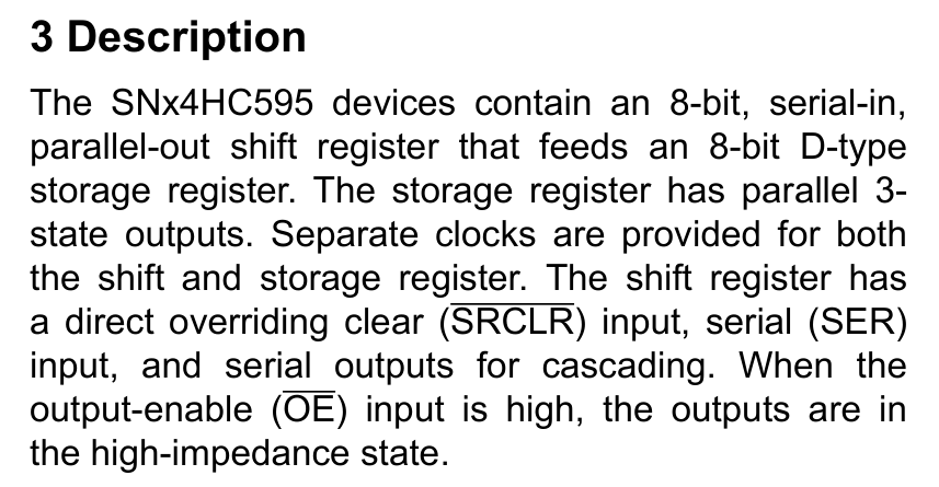
Sometimes it takes a few passes to understand what the description is saying, especially if you don’t know what a shift register is or how a 3-state buffer works. Here, I’ll go sentence-by-sentence to explain each detail, but after awhile I should be able to understand at a glance what the part does, as well as something about how it works. 5
-
an 8-bit, serial-in, parallel-out shift register: The general classification of the 74595 is a register: it functions as memory, storing information for later access. If you’ve studied CPUs in any detail before, the word sounds familiar: processors use processor registers to quickly store and read information when performing machine instructions. Hardware registers are a special type of memory: in addition to storing information, they also perform some specific function. Here, the 74595 is a shift register: it stores 8 bits of information, and each time it receives a new bit of data, it shifts its current data one spot to the right. This is equivalent to
>> 1, bit wise shifting right by 1 in C, orSHR 1, %raxin AT&T syntax x86 assembly.Shift registers can have serial and parallel inputs and outputs, which leads to four types of shift registers: serial-in, serial-out (SISO), serial-in, parallel-out (SIPO), parallel-in, serial-out (PISO), and parallel-in, parallel-out (PIPO). Serial data is sent one bit at a time over a single line of communication: hence, a register with serial input has only one data input pin. Parallel data is sent at the same time across multiple pins. Since the 74595 is an 8-bit register, it has 8 parallel outputs, plus a 9th output used to add more shift registers (known as “daisy-chaining”).
Source: Wikimedia Commons
-
feeds an 8-bit D-type storage register: At the transistor level, memory is stored in flip-flops and latches. The main difference between the two is that flip-flop state changes are triggered by a clock signal, while latch changes are asynchronous and can change state at any time. A D-type (data) flip-flop has one input, and its output matches the input on each clock edge.
The distinction implies that our shift register is actually made up of two registers: a shift register to hold and shift input values, and a storage register to hold output values. The shift and output registers form a pipeline, and a clock is used to trigger the output register’s outputs.
Source: Wikimedia Commons
-
Separate clocks are provided for both the shift and storage register: A clock exists for the storage register. It uses D flip-flops, which are controlled by a clock and allow. Why does a separate clock exist for the shift register?
Consider the following question: when should the shift register shift its input? The shift register could shift on every input, but suppose it get a string of low inputs. How does it know to track a distinct low input? Tracking inputs requires some mechanism (a clock) to “tick” every time it records a new input state and shifts its current state over by 1 bit to make room.
This clock is distinct from the clock to output data to allow time for data to flow from the shift register to the storage register and ensure stable data. Distinct clocks also give the circuit designer finer control over how the IC is used. However, the data sheet also mentions (on pg. 6) that the clocks can be tied together - if they are, the shift register is always one clock pulse ahead of the storage register.
-
The storage register has parallel 3-state outputs: Another logic component in digital circuits is the tri-state buffer (or three-state buffer). This buffer has two inputs and one output. Normally, the output buffer would have two possible states: high (1) or low (0), dictated by its input. However, a tri-state buffer’s second input triggers a third state: high impedence.
-
When the output-enable (OE) input is high, the outputs are in the high-impedance state: Normally, it might be preferred to just display whatever output is stored in the register. If the second input (called output enable, or OE, by Texas Instruments) of the tri-state buffer is low, this is what happens. When OE is set high, a valve is turned off, and the output doesn’t have enough current to register anything. The current is impeded by the output enable being set high, regardless of whether the current is low or high.
The notes linked above use a helpful analogy: imagine that high current is one color (red), low current is another color (black), and no current is no color. When the OE pin is set low, the output buffer displays the input pin’s color. The circuit is complete, and the color “flows through”. When the OE pin is high, the valve is closed, the output buffer is blocked, and no color can flow through.
One use case of tri-state buffers is when writing output to a bus. The high-impedence state provides control over what data makes it onto the bus, and what data is blocked from the bus.
-
The shift register has a direct overriding clear (SRCLR) input, serial (SER) input, and serial outputs for cascading: Above, I’ve already covered four of the 74595’s input pins. The serial input (SER) is used to provide input data to the register. The serial clock (SRCLK) is the clock that triggers when the shift register shifts and accepts a new input. The storage register clock (RCLK) updates the output register. The output enable (OE), when high, cuts off any output current from the output register. The fifth pin, mentioned here, is the direct overriding clear (SRCLR), which overrides all current register values and sets them low.
The phrase also mentions a new feature: serial outputs for cascading. From the first sentence of the description, it is known that the register produces an 8-bit parallel output; however, I mentioned that a 9th existed. This output pin is a serial line that outputs the last bit of the shift register, the one being bumped off. It can be connected to the serial input pin of, say, another shift register to allow for outputs longer than 8 or 9 bits.
The first page of the datasheet also contains a number of features. Several of these are part of the description, but others provide specific measurements and capabilities that help characterize this implementation of the 595 shift register. These features range from operating specifications (“Wide operating voltage range of 2 V to 6 V”, “Low input current: 1 μA (maximum)") to output capabilities. One notable feature is that “High-current 3-state outputs can drive up to 15 LSTTL loads”. Translated, each output pin can provide enough current to drive multiple low-powered TTL devices, a feature especially useful in larger circuits.
The circuits built later in this post use LEDs, so it’s important to note the output current drive (“±6-mA output drive at 5 V”) and use the correct resistors to match (something I did not do at first).
Pin configuration
Often, the pin configuration is the first section of a datasheet that you’ll look at. For example: you have an 8-bit AND gate and want to know which pins connect to power (VCC) and ground (GND), and where the inputs and outputs are. The function of the IC is not a mystery, but where to hook up the wires is.
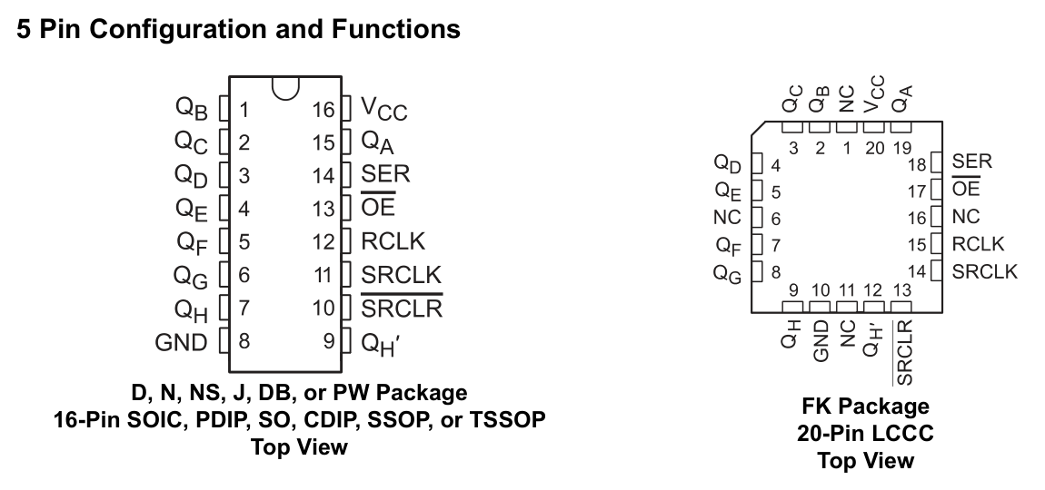
Two pin configurations are shown. The package of the 74HC595N (the last letter of the IC’s name), determines whether to use the 2-row rectangular diagram or the 20-pin square (e.g., a SN74HC595FK).
Since the SN74HC595N is a PDIP package, the left diagram is relevant. On the IC, there are the five input pins, nine output pins ($\text{Q}_A$ through $\text{Q}_H$, plus the serial output pin $\text{Q}_H'$), and connections to power and ground. Pins 1 and 16 are located next to the side indent in the chip.
Block diagram
Page 11 of the datasheet has an enlarged view of the functional block diagram from the first page.
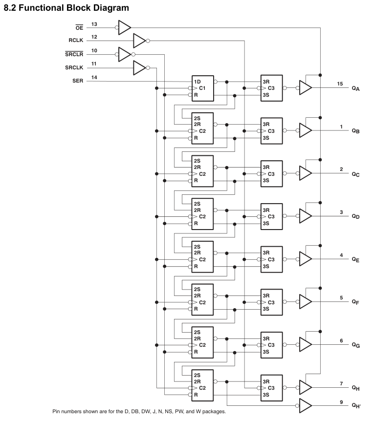
Integrated circuits are themselves typically made up of smaller components, such as logic gates and flip flops. Functional block diagrams model the system as a whole by abstracting each smaller component into a symbol. In this diagram, the three main areas detailed (from left to right) are the shift register, the storage register, and the tri-state bus. The diagram breaks up each of these components into its sub components: the shift register is made up of mostly dual D-type flip-flops, the storage register is D-type flip-flops, and the tri-state bus is tri-state buffers.
A block diagram can be thought of as a logical schematic: it abstracts away the electrical components to focus on how information flows through the system. What happens when the serial clear pin is set high? What components are updated by the register clock?
In the block diagram above, let’s examine the first row.

The first row contains two D-type flip-flops storing one bit each. The first flip-flop is one of the eight bits stored by the shift register, while the second is the first of eight bits stored by the storage register. The triangle on the right represents a tri-state buffer. This is distinct from the four triangles for the first four inputs (OE, RCLK, SRCLR, and SRCLK), which represent NOT gates.
The three inputs to the first flip-flop are SER (serial input - the main data line), SRCLK (the clock for the shift register), and SRCLR (the signal to reset the register). The empty circles represent NOT gates for bit inversions, while the filled-in circles represent connection points where signals meet and branch. Inside of the two D-type flip-flops, there is a triangle, which signifies that the clock is edge-triggered. See “Timing Diagrams” for why both flip-flops are positive edge-triggered.
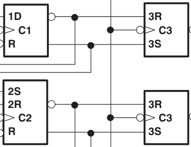
Inside of each flip-flop, the inputs are labeled. The letters represent the type of signal sent.
- C: clock input
- D: data input
- R: reset input
- S: set input (complement to reset)
The numbers represent the stages of the shift register. Shift registers are sequential - you shift one bit at a time, in a given ordering (0 -> 1 -> 2 …). Each flip-flop and tri-state buffer represents a stage in the sequential process, depending on where it is located in the circuit. The textbook at the link above has a good explanation of how a four stage shift register works, and how each stage interacts with the stage before it and the one after.
The 74HC595 has three main stages shown in the diagram: the input stage (1D), the subsequent shift register stages (2D), and the storage register stage (3R/3S). The datasheet describes how the stages link to the possible functions of the shift register:
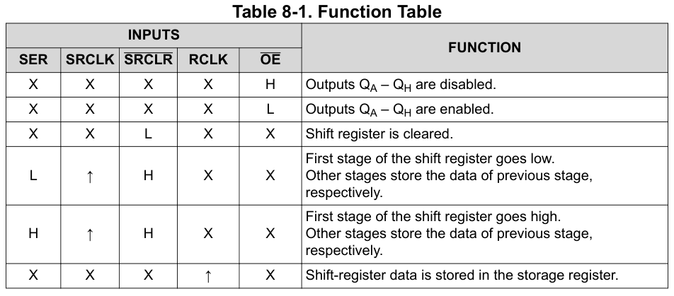
The first stage always takes input from SER, while every other stage takes its input from the previous stage. The subsequent bits are all treated as one stage (2D, 3S/3R) because they all function identically in shifting data forward.
Note how R has no number next to it - reset is a control signal that affects all stages immediately (not sequentially). Note that SRCLR affects all bits in the shift register simultaneously, but not the storage register; hence the storage register is updated sequentially (when RCLK triggers).
To set the first bit of output for the shift register as a 1, we first set SER and SRCLR high. The bar over SRCLR indicates that by setting SRCLR high, we are performing the inverse action: high for normal operation, low for clear. After setting SER and SRCLR high, we next pulse the SRCLK pin (set to high, then low). The clock impulse is triggered on the transition from low to high (positive edge), capturing the input data and updating the flip-flop’s output. 6
To send the bit in the first D flip-flop of our shift register to the corresponding output pin ($\text{Q}_A$), we first set OE (output enable) to active low. The bar above OE indicates that when we set it to low, the current goes high into the tri-state buffer and allows the output through with no impedance. The output is triggered by transitioning RCLK from low to active high, and with OE low, the output value now appears at the pin $\text{Q}_A$.
Timing diagram
When manipulating a shift register at human speeds, the timing specification is less relevant - we operate at the scale of seconds and tens or hundreds of milliseconds ($10^{-3}$ s), not nanoseconds ($10^{-9}$ s). However, shift registers are often used in conjunction with other integrated circuits that operate much faster: CPUs.
The guaranteed maximum operating frequency of the SN74HC595 is 29 MHz, while under normal laboratory conditions ($\text{T}_{\text{A}}$) it operates at 42 MHz. This is slower than many microcontrollers 7, such as the STM32F446 used later (with a CPU frequency up to 180 MHz, and an I/O frequency up to 90 MHz). Many modern CPUs also operate at a much faster speed, retiring more than one instruction per nanosecond. The difference in operating frequencies matters when putting together a system comprised of different ICs, such as an I2C bus.
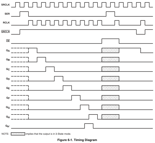
The timing diagram above illustrates the timing and switching durations in an abstracted format, similar to how the block diagram abstracts away the internal circuitry to leave functional components. 8 You can watch the single bit of input get shifted right to each output register as time increases (as you move right).
You might notice that the shift register clock (SRCLK) and storage register clock (RCLK) alternate between pulses. The diagram provides a logical structure to the input and output transitions - it doesn’t indicate that the waveforms shown are precisely how those clocks work during operation. It illustrates what was mentioned in the previous section - the inputs and outputs are positive-edge triggered. More explicitly, in Section 8.1:
Both the shift register clock (SRCLK) and storage register clock (RCLK) are positive-edge triggered. If both clocks are connected together, the shift register always is one clock pulse ahead of the storage register.
Positive-edge triggered means that the output changes as the clock transitions from low to high (the “positive edge” of the waveform). You can see that the first time RCLK goes high, the output appears on the output pin $\text{Q}_A$.
Note from the table in section 6.6 how the minimum timing requirements get lower as the operating voltage increases.

When a current is switched from high to low, the waveform is not square or immediate. In reality, switching from high to low is on a spectrum, depending on characteristics such as signal dampening, the materials used, and other considerations. As you improve this transformation, your waveform improves and becomes more square. Increasing the voltage supplied to the shift register forces the signal to settle faster, and therefore the time requirements to wait for the transition are lower.
Source: Wikimedia Commons
There are two separate sections concerned with timing - “Timing Requirements” and “Switching Characteristics”. The two are related, but measure different things. Timing refers to how long a pulse must last (at a minimum) before another signal can be sent. Switching refers to the duration between a change in an input signal and the change in the corresponding output signal.
A good example of switching is what happens when output enable (OE) is transitioned from active low to high. From what we learned earlier, a positive transition in OE activates a high-impedence state, preventing any signal from being sent by the register’s output pins. Based on the datasheet, there are three times associated with OE being triggered:
- $\text{t}_\text{en}$ (50 pF): enabling OE (low -> high)
- $\text{t}_\text{dis}$ (50 pF): disabling OE (high -> low)
- $\text{t}_\text{en}$ (150 pF): enabling OE (low -> high at higher capacitance)
The first $\text{t}_\text{en}$ has a “typical” switching time of 13 ns and a max switching time of 26 ns. It will take at most 26 nanoseconds for the output pins to enter a state of high impedence from when the OE pin crosses the 50% threshold from low to high ($\text{t}_\text{PLZ}$/$\text{t}_\text{PHZ}$ in the diagram below).
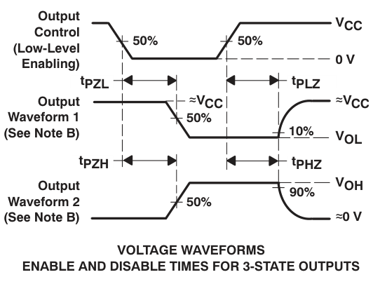
The diagram above is the waveform for the tri-state buffer abstracted away by the timing diagram. It is still an abstraction (the signal does not travel in straight lines), but it is more accurate. It provides timing information for triggering the output enable (OE) pin.
The first waveform is for OE. The pin starts at high (a state of impedance), transitions to low, then back to high. The other two waveforms represent output pins. Waveform 1 is when the output pin is supposed to be active low ($\text{V}_\text{OL}$). It starts in an unknown state (hence the $\approx$ symbol next to $\text{V}_\text{CC}$), transitions to its expected state when enabled, then goes back to an unknown state of impedance. You can see the times clearly indicated by the distance between dashed lines - each dashed line is when one of the waveforms reaches the 50% mark on the waveform, the transition point.
Specifications
This is arguably the most important section when it comes to designing a circuit that uses an IC. However, I will wait until Part 2 to cover this in more depth.
First circuit: 16-LED
I built my first circuit with no microcontroller - just human inputs.
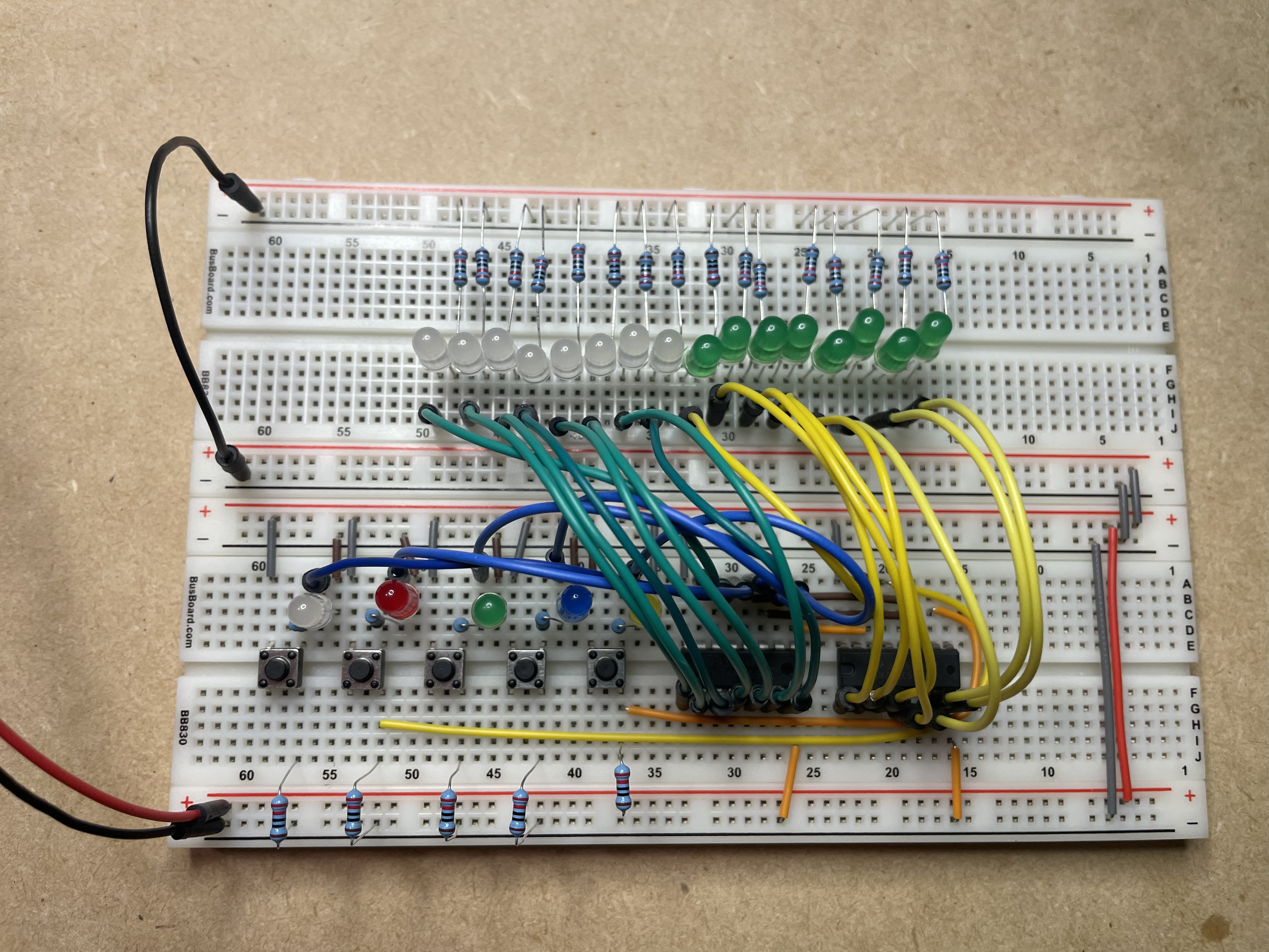
In the bottom left corner are five buttons with corresponding LEDs. 9 Each button controls one of the five inputs to the shift registers:
- White: SER
- Red: OE
- Green: RCLK
- Blue: SRCLK
- Yellow: SRCLR
Four of them are tied to ground, but the button on the right (SRCLR) is tied to power. Since SRCLR is inverted, we only want it to go high when clearing the registers. If it was not inverted, we would hold it low, like the other inputs, but because of the inversion we hold it high.
The blue wires connect the input to the first shift register, and the green wires connect the output from the register to the first eight output LEDs (white). The inputs are tied into the second shift register through flat jumper wires (some above, some below), and that register’s outputs are connected to the green LEDs through the yellow jumper wires.
To turn the first LED on (output $\text{Q}_A$), SRCLK must register while SER is on. In terms of pressing buttons, this corresponds to holding the white LED while pressing the blue LED. The shift register is triggered on the press of the button, not its release. To send the to the output LEDs, RCLK (green) is pressed.
To shift the output right, we can send a series of SRCLK inputs while SER is not pressed, shifting the ‘1’ bit over a few places. The display is triggered by pressing RCLK again.
By default, OE is low. Since it is inverted (the bar over OE), it is always high, allowing output through the tri-state buffer unimpeded. Pressing the red button sets OE to high and puts the outputs in a state of high impedance.
To clear the register, press the SRCLR button (yellow) and then RCLK. SRCLK doesn’t need to be triggered - the SRCLR input is unphased and clears the shift register immediately.
Using an MCU
One way to maximize the potential of the above circuit is to send inputs faster using microcontroller units (MCUs). I next used an Arduino Uno (ELEGOO, with an ATMega328P processor) to count on a seven-segment display, and an STM32F446 to control the LEDs in the circuit above.
Schematic with Arduino Uno
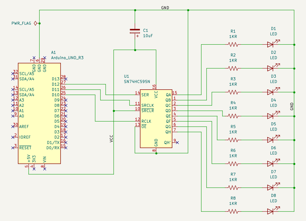
Adding a microcontroller into the circuit isn’t difficult. The schematic below shows how adding an Arduino Uno to a circuit with one shift register requires tying three data output pins to control the serial input and both clocks. The other two inputs (SRCLR, OE) are connected to their respective defaults.
Circuit 2: Seven-segment display with Arduino UNO (ATMega328P)
Online, one program people often write using shift registers is counting to $2^{16}\space (65536)$. I decided instead to count to 16 using a seven-segment display.
You can the full circuit at 0:12 in the video. The UNO controls power and ground, the black and red wires at the bottom. It also controls the clock inputs (RCLK, SRCLK) using the output ports connected with the long white and black wires, and the input with the red wire. Output from the SN74HC595N is sent through registers and ends up at the display.
Normally, this display would require eight GPIO pins from the Arduino; however, using the SN74HC595N, we only needed three. This is the main reason this IC is included in beginner’s electronic kits. People often start by lighting up LEDs when using MCUs; “Blinky” is the “Hello World” in this way. Shift registers provide a convenient way to blink many LEDs while using less IO ports.
Circuit 3: 16-LED with STM32
One program I saw others do that looked fun was bouncing a pulse through the LEDs as a wave. Another was to use PWM (pulse width modulation) to control how bright the LEDs shone. I combined these two into one program running on a Nucleo board (STM32F4 processor).
I used STM32CubeIDE’s HAL (hardware abstraction layer) to write the program; however, I didn’t like their implementation of PWM (designating specific pins and setting them up for PWM), so I wrote my own function to do the same: 10
// Define PWM macros
#define NUM_LEDS 16
#define WAVE_DELAY 30
#define PWM_STEPS 100
#define PWM_PERIOD 100  // Number of microseconds for one PWM period

/**
 * (Doxygen generated by Claude Sonnet 3.5 to explain function in detail)
 *
 * @brief PWM for 16 LEDs using shift registers
 *
 * @details This function implements PWM by repeatedly writing to
 * the shift registers for a specified number of cycles. During the
 * "on" portion of the PWM cycle, it writes the actual LED bit
 * pattern. During the "off" portion, it writes zeros.
 *
 * The function uses three control pins:
 * - SER: Serial data input
 * - SRCLK: Shift register clock
 * - RCLK: Storage register clock (latch)
 *
 * The timing is controlled by:
 * - PWM_PERIOD: Total period length (100 cycles)
 * - pwm_duty: Determines what portion of the period the LEDs are on
 *
 * @param bits 16-bit pattern where each bit represents one LED
 *        (1 = on, 0 = off)
 * @param pwm_duty PWM duty cycle (0-100), where 0 is always off
 *        and 100 is always on
 *
 * @note This function blocks for the duration of one PWM period
 * @note The shift register reads bits LSB first
 */
void pwm_write(const uint16_t bits, const uint8_t pwm_duty) {
	uint8_t on_cycle = (PWM_PERIOD * pwm_duty) / 100;
	uint8_t off_cycle = PWM_PERIOD - on_cycle;

	for (int j = 0; j < PWM_PERIOD; ++j) {
		for (int i = 0; i < NUM_LEDS; ++i) {
            if (j < on_cycle)
			    HAL_GPIO_WritePin(SER_GPIO_Port, SER_Pin, (bits>>i) & 1);
			else
                HAL_GPIO_WritePin(SER_GPIO_Port, SER_Pin, 0);
            HAL_GPIO_WritePin(SRCLK_GPIO_Port, SRCLK_Pin, GPIO_PIN_SET);
			HAL_GPIO_WritePin(SRCLK_GPIO_Port, SRCLK_Pin, GPIO_PIN_RESET);
		}
		HAL_GPIO_WritePin(RCLK_GPIO_Port, RCLK_Pin, GPIO_PIN_SET);
		HAL_GPIO_WritePin(RCLK_GPIO_Port, RCLK_Pin, GPIO_PIN_RESET);
	}
}
STM32CubeIDE generates a lot of template code to set the ARM-M4 processor up
correctly, similar to how ArduinoIDE abstracts away how a program is loaded onto
its processor. Within CubeIDE’s generated code are USER CODE sections that
aren’t altered when regenerating code. main.c has a while (1) loop with one
of these sections where I implemented the program for this circuit.
/* Infinite loop */
while (1)
{
    int spins, i;

    // wave
    for (spins = 0; spins < 5; ++spins) {
  	  for (i = 0; i < num_bits; ++i) {
  		  pwm_write(1 << i, 100);
  		  HAL_Delay(WAVE_DELAY);
  	  }

  	  for (i = num_bits - 2; i > 0; --i) {
  		  pwm_write(1 << i, 100);
  		  HAL_Delay(WAVE_DELAY);
  	  }
    }

    // pwm
    uint16_t all_on = 0xFFFF;

    pwm_write(0, 100);
    HAL_Delay(100);

    for (int i=0; i<=90; i++) {
  	  uint32_t start = HAL_GetTick();
  	  while(HAL_GetTick() - start < 15) {
  		  pwm_write(all_on, i);
  	  }
    }

    for (int i=90; i>=0; i--) {
  	  uint32_t start = HAL_GetTick();
  	  while(HAL_GetTick() - start < 15) {
  		  pwm_write(all_on, i);
  	  }
    }
    HAL_Delay(100);
}
One thing you’ll notice in the videos above is how bright the LEDs are. This is because I used the wrong resistors. $220\space\Omega$ resistors are typically used when considering the forward voltage of an LED, but the shift register has maximum ratings in the specification that the LED exceeds with this resistor. 11
To get the correct resistance required, we can apply Ohm’s law. With a $220\space\Omega$ resistor, and assuming a $2\space\text{V}$ drop per LED, each LED draws $(5 - 2)/220 = 13.6\space\text{mA}$ of current. With $8$ LEDs, this adds up to $109.1\space\text{mA}$ of current, well above the maximum output rating of $70\space\text{mA}$ for the SN74HC595N.
Using a $1\text{K}\space\Omega$ resistor, we can lower the current draw to $24\space\text{mA}$, enough to light each LED but not so much that the register burns out.
I quickly added stronger resistors ($1\text{K}\space\Omega$) to reduce the current draw of the LEDs and avoid burning out the shift registers; however, none of the videos or images above have those circuits.
Further reading
This section will soon include Part 2 of this post. In that, I will go into sections of the datasheet I haven’t covered yet, such as the specifications, “typical characteristics” graph, and application layout information.
I’ll also build more circuits: one uses only one GPIO output port for data (instead of three), and another will output data onto a bus using a shift register.
This post was meant as an introduction to reading datasheets, understanding shift registers, and building circuits with it. The purpose of the second post is to solve the mystery: what exactly are the applications of the 74HC595N in systems today? How is it used in the devices below?

One is obvious; the others less so.
Resources & external links
Some of the most useful and interesting references I used when writing this post are listed and linked below.
- The datasheet of the SN74HC595N, courtesy of Texas Instruments. TI also has a helpful guide on how to read datasheets
- Don Lancaster’s TTL and CMOS cookbooks
- An in-depth video explaining shift registers with an Arduino UNO (and its associated article
- A simple & straightforward demonstration of how to use a shift register. I based my first circuit on this implementation
- A very cool use of the 74HC595
Thank you to Eric Hazen for helps with explaining several basics of electronics and physics necessary for this post.
Thank you also to Ben Eater and Mitch Davis. Their videos of related concepts inspired this post.
-
The link might lead to no parts, depending on when you click it. ↩︎
-
The 74850 and 74851 are no longer active on TI’s site, but you can find them at DigiKey. ↩︎
-
When designing circuits on KiCAD, it took me a minute to realize that I wanted the package sizing information, not the IC-specific information for pins (what matters is where they’re located on the PCB, not what they do). One important point to make is that the “Device Information” size given is nominal - the physical footprint size is what matters.
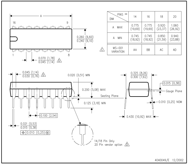 If you look
closely at the diagram, you’ll notice that the nominal width from the
datasheet (6.35 mm) is different from the actual width (7.94 mm). Both are
taken by averaging the range provided. When designing a PCB, use the actual
size so that the part fits into the holes properly. ↩︎
 -
The principle of relying on primary sources does not apply solely to datasheets. When writing software, past a certain point, one needs to learn to use the resources available; however, there are many ways to do this. Asking questions and learning things on your own is a skill that requires practice.
At first, I was going to go on a tangent about how telling someone “RTFM” is the kindest thing you can do for them. While I do believe this to some extent, I have come to understand that reading the manual requires someone understanding of the software/program/device in question first, which comes from experience, textbooks, guides, and others. People need to be able to learn how to help themselves when solving their own problems. However, it doesn’t make sense to tell someone to read themanpage onlsif they don’t know what amanpage is, or to “read the documentation” without providing documentation that answers the question.
I don’t understand much about integrated circuits, but spending more time than necessary reading the datasheet has taught me more than just how to fan output to multiple LEDs with the 74HC595N. ↩︎ -
This is the equivalent of a “Hello world” program with comments on every line. ↩︎
-
To see this in action, check out this graphic. To learn more about flip-flops in general, I recommend any number of YouTube videos, the Wikipedia page, or GraphicMaths. ↩︎
-
Not the Arduino UNO! With an ATMega328P processor, this board achieves a maximum CPU speed of 16 MHz, below the minimum guaranteed operating frequency of the SN74HC595. By default, the processor runs at 1 MHz - even slower than the shift register. None of these measurements take into account the difference between CPU and I/O pin frequency, either. ↩︎
-
rectangle : D-type flip-flop :: square wave : actual waveform ↩︎
-
Unfortunately, none of the buttons are debounced. This makes it tricky when you want to perform a specific action, such as “light up every other LED”. ↩︎
-
I thought annotating this function would be in the same spirit of the rest of this post, as every aspect of this post has been detailed so far. ↩︎
-
Again, the specifications section of the datasheet is arguably the most important when it comes to avoiding destroying your components - I’ll cover that in the next post. ↩︎